Samsung Starts Mass Production of 16Gb GDDR6 Memory ICs with 18 Gbps I/O Speed
by Anton Shilov on January 18, 2018 9:00 AM EST
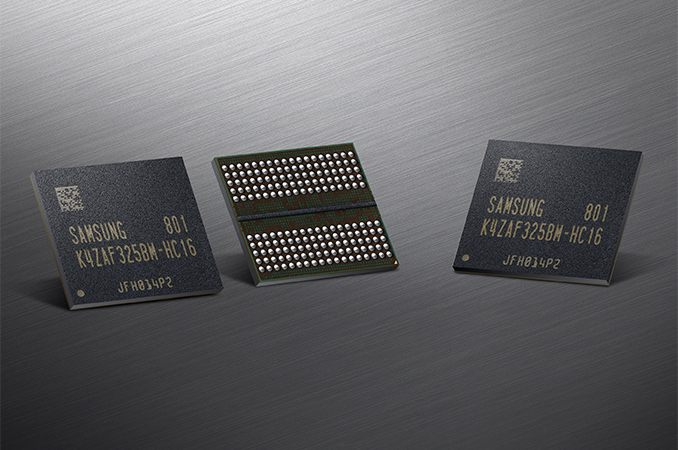
This week, Samsung has announced that it has started mass production of its GDDR6 memory chips for next-generation graphics cards and other applications. The new chips will be available in 16 Gb densities and will feature an interface speed that is significantly higher when compared to that of the fastest GDDR5 and GDDR5X ICs can offer.
GDDR6 is a next-generation specialized DRAM standard that will be supported by all three leading makers of memory. Over time, the industry will introduce a great variety of GDDR6 ICs for different applications, performance and price requirements. What Samsung is announcing this week is its first 16 Gb GDDR6 IC that features an 18 Gbps per pin data transfer rate and offers up to 72 GB/s of bandwidth per chip. A 256-bit memory subsystem comprised of such DRAMs will have a combined memory bandwidth of 576 GB/s, whereas a 384-bit memory subsystem will hit 864 GB/s, outperforming existing HBM2-based 1.7 Gbps/3092-bit memory subsystems that offer up to 652 GB/s. The added expense with GDDR6 will be in the power budget, much like current GDDR5/5X technology.
| GPU Memory Math: GDDR6 vs. HBM2 vs. GDDR5X | ||||||||
| Theoretical GDDR6 256-bit memory sub-system | Theoretical GDDR6 384-bit memory sub-system | NVIDIA Titan V (HBM2) |
NVIDIA Titan Xp |
NVIDIA GeForce GTX 1080 Ti | NVIDIA GeForce GTX 1080 | |||
| Total Capacity | 16 GB | 24 GB | 12 GB | 12 GB | 11 GB | 8 GB | ||
| B/W Per Pin | 18 Gb/s | 1.7 Gb/s | 11.4 Gbps | 11 Gbps | ||||
| Chip capacity | 2 GB (16 Gb) | 4 GB (32 Gb) | 1 GB (8 Gb) | |||||
| No. Chips/KGSDs | 8 | 12 | 3 | 12 | 11 | 8 | ||
| B/W Per Chip/Stack | 72 GB/s | 217.6 GB/s | 45.6 GB/s | 44 GB/s | ||||
| Bus Width | 256-bit | 384-bit | 3092-bit | 384-bit | 352-bit | 256-bit | ||
| Total B/W | 576 GB/s | 864 GB/s | 652.8 GB/s | 547.7 GB/s | 484 GB/s | 352 GB/s | ||
| DRAM Voltage | 1.35 V | 1.2 V (?) | 1.35 V | |||||
The new GDDR6 architecture enables Samsung to support new and higher data transfer rates with non-esoteric memory form factors. To increase the interface speed, GDDR6 memory was redesigned both internally and externally. While details about the new standard will be covered in a separate article, two key things about the new memory tech is that GDDR6 features a x8/x16 per-channel I/O configuration, and each chip now has two channels. By contrast, GDDR5/GDDR5X ICs feature a x16/x32 I/O config as well as one channel per chip. While physically GDDR6 chips continue to feature a 16-/32-bit wide bus, it now works differently when compared to prior generations (as it consists of two channels).
In addition to higher performance, Samsung’s GDDR6 16 Gb chips also operate at 1.35 V voltage, down 13% from 1.55 V required by high-performance GDDR5 ICs (e.g., 9 Gbps, 10 Gbps, etc.). According to Samsung, the lowered voltage enables it to lower energy consumption of GDDR6 components by 35% when compared to ultra-fast GDDR5 chips. Samsung attributes lowered voltage to its new low-power circuit design. Meanwhile, based on information we know from Micron and SK Hynix, their GDDR6 DRAMs will also operate at 1.35 V.
Samsung uses one of its 10nm-class process technology to produce its GDDR6 components. The company claims that its 16 Gb ICs bring about a 30% manufacturing productivity gain compared to its 8 Gb GDDR5 chips made using its 20 nm process technology. Typically, Samsung’s productivity gain means increase in the number of chips per wafer, so the company has managed to make its 16 Gb ICs smaller than its previous-gen 8 Gb ICs. The company does not elaborate on its achievement, but it looks like the new chips are not only made using a thinner process technology, but have other advantages over predecessors, such as a new DRAM cell structure, or an optimized architecture.
Samsung’s 16 Gb GDDR6 chips come in FBGA180 packages, just like all industry-standard GDDR6 memory components from other manufacturers.
Samsung did not disclose when it plans to ship its GDDR6 DRAMs commercially, but since it had already started mass production, it is highly likely that the company’s clients are ready to build products featuring the new memory.
Related Reading
- Micron Finishes GDDR6 Internal Qualification, Eyes H1'2018 Mass Production
- Samsung Starts Production of 8 Gb DDR4-3600 ICs Using 2nd Gen 10nm-Class Tech
- Samsung Pre-Announces 16 Gbps GDDR6 Chips for Next-Gen Graphics Cards
- Micron Discusses GDDR: 16 Gbps GDDR5X, 16 nm GDDR6 and GDDR5
- SK Hynix Advances Graphics DRAM: GDDR6 Added to Catalogue, GDDR5 Gets Faster
Source: Samsung


24 Comments
View All Comments
Pork@III - Thursday, January 18, 2018 - link
Theoretical GDDR6 256-bit memory sub-system Theoretical GDDR6 384-bit memory sub-systemThat is awesome! But....Why don't NVIDIA and AMD make 512 and 448 bit cards today?
T1beriu - Thursday, January 18, 2018 - link
Overkill? Crazy power consumption? increased die sizes?nevcairiel - Thursday, January 18, 2018 - link
Because it costs a whole lot of money and die space, and while more memory bandwidth can help various workloads, there is also limits to how much it can.Pork@III - Thursday, January 18, 2018 - link
Okay, and 10+ years ago, how it was not a problem to offer 512-bit video cards. Was it easier and cheaper to manufacture? At that, prices were not higher than the current flagship models (from before the mining speculation). I do not accept explanations like yours for a good enough argument.DanNeely - Thursday, January 18, 2018 - link
No, they did it because they desperately needed the extra bandwidth or total capacity for top end GPUs. Doing so added a lot to manufacturing costs, in the number of ram chips, number of PCB layers to connect them, and higher manufacturing failure rates. Since then ram makers have managed to provide ram that is fast enough and high enough capacity that going that wide hasn't been necessary.Adding more ram/a wider bus than the GPU can utilize wouldn't do anything but make the card more expensive; and other than AMDs 1st generation HMB1 cards nothing at the high end in the last decade has been ram limited.
MrSpadge - Thursday, January 18, 2018 - link
And also back then the wider memory busses increased chip costs (area) and power consumption over more narrow, similarly clocked choices. The chip area was cheaper back then, though.Dragonstongue - Thursday, January 18, 2018 - link
because it takes ALOT of die space for the extra wide memory bus, which drives up cost and complexity a great deal, and, the "modern" designs seem to favor square numbers 128-256-512, seems most of the not square number cards while they can be fast do not seem to get the proper scaling in some things..as the maker AMD Nvidia or whatever need to "feed the card" properly, so a massive or tiny bus not being fed with fast enough memory or whatever makes using it, useless and expensive a proposition.am sure sometimes they do such on purpose to make sure they can market at a higher price then should but usually they are building them to effectively use a "narrow" but fast memory bus, obviously always exceptions to the rule, such as many many many cards loaded with a whole whack of gb of memory they can never ever use because of a narrow bus or simply not enough grunt behind the design.
Pork@III - Thursday, January 18, 2018 - link
I think they just save costs in order to maximize their net profit. This action brings us to the fact that we are receiving less and less benefits for the money we spend.MrSpadge - Thursday, January 18, 2018 - link
If they introduced a card with lacked memory bandwidth, it would underperform and could not be sold for the target price. Hint: any company doing this is already bankrupt.And yes, the more narrow busses increase the companies profit - but not at the cost of performance. That's why overclocking GPU memory helps performance a bit, but overclocking the chip yields far greater gains, percentage-wise. That means the cards are well balanced and have approximately enough bandwidth.
Frenetic Pony - Thursday, January 18, 2018 - link
Nvidia doesn't have the design for it, which would be massive overkill when it comes to filling up the rest of the die with enough power to make use of it anyway. AMD did at one point, but switched to HBM, which Nvidia has done as well, at least for their big cards.Thing is, while HBM is more efficient from die size/bandwidth and energy used, it's also turned out to be too limited and expensive right now. So here's GDDR6, less efficient than HBM2, and far less than 3 (whever that comes out). But easier to make, and so cheaper and more available. Considering the ridiculous price you have to pay for a GPU today, assuming you can even get one at all, cheaper and more available is definitely preferred right now.