NVIDIA's Fermi: Architected for Tesla, 3 Billion Transistors in 2010
by Anand Lal Shimpi on September 30, 2009 12:00 AM EST- Posted in
- GPUs
Architecting Fermi: More Than 2x GT200
NVIDIA keeps referring to Fermi as a brand new architecture, while calling GT200 (and RV870) bigger versions of their predecessors with a few added features. Marginalizing the efforts required to build any multi-billion transistor chip is just silly, to an extent all of these GPUs have been significantly redesigned.
At a high level, Fermi doesn't look much different than a bigger GT200. NVIDIA is committed to its scalar architecture for the foreseeable future. In fact, its one op per clock per core philosophy comes from a basic desire to execute single threaded programs as quickly as possible. Remember, these are compute and graphics chips. NVIDIA sees no benefit in building a 16-wide or 5-wide core as the basis of its architectures, although we may see a bit more flexibility at the core level in the future.
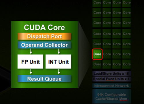
Despite the similarities, large parts of the architecture have evolved. The redesign happened at low as the core level. NVIDIA used to call these SPs (Streaming Processors), now they call them CUDA Cores, I’m going to call them cores.

All of the processing done at the core level is now to IEEE spec. That’s IEEE-754 2008 for floating point math (same as RV870/5870) and full 32-bit for integers. In the past 32-bit integer multiplies had to be emulated, the hardware could only do 24-bit integer muls. That silliness is now gone. Fused Multiply Add is also included. The goal was to avoid doing any cheesy tricks to implement math. Everything should be industry standards compliant and give you the results that you’d expect.
Double precision floating point (FP64) performance is improved tremendously. Peak 64-bit FP execution rate is now 1/2 of 32-bit FP, it used to be 1/8 (AMD's is 1/5). Wow.
NVIDIA isn’t disclosing clock speeds yet, so we don’t know exactly what that rate is yet.
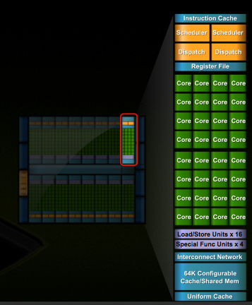
In G80 and GT200 NVIDIA grouped eight cores into what it called an SM. With Fermi, you get 32 cores per SM.

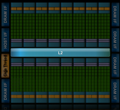
The high end single-GPU Fermi configuration will have 16 SMs. That’s fewer SMs than GT200, but more cores. 512 to be exact. Fermi has more than twice the core count of the GeForce GTX 285.
| Fermi | GT200 | G80 | |
| Cores | 512 | 240 | 128 |
| Memory Interface | 384-bit GDDR5 | 512-bit GDDR3 | 384-bit GDDR3 |
In addition to the cores, each SM has a Special Function Unit (SFU) used for transcendental math and interpolation. In GT200 this SFU had two pipelines, in Fermi it has four. While NVIDIA increased general math horsepower by 4x per SM, SFU resources only doubled.
The infamous missing MUL has been pulled out of the SFU, we shouldn’t have to quote peak single and dual-issue arithmetic rates any longer for NVIDIA GPUs.
NVIDIA organizes these SMs into TPCs, but the exact hierarchy isn’t being disclosed today. With the launch's Tesla focus we also don't know specific on ROPs, texture filtering or anything else related to 3D graphics. Boo.
A Real Cache Hierarchy
Each SM in GT200 had 16KB of shared memory that could be used by all of the cores. This wasn’t a cache, but rather software managed memory. The application would have to knowingly move data in and out of it. The benefit here is predictability, you always know if something is in shared memory because you put it there. The downside is it doesn’t work so well if the application isn’t very predictable.
Branch heavy applications and many of the general purpose compute applications that NVIDIA is going after need a real cache. So with Fermi at 40nm, NVIDIA gave them a real cache.
Attached to each SM is 64KB of configurable memory. It can be partitioned as 16KB/48KB or 48KB/16KB; one partition is shared memory, the other partition is an L1 cache. The 16KB minimum partition means that applications written for GT200 that require 16KB of shared memory will still work just fine on Fermi. If your app prefers shared memory, it gets 3x the space in Fermi. If your application could really benefit from a cache, Fermi now delivers that as well. GT200 did have an L1 texture cache (one per TPC), but the cache was mostly useless when the GPU ran in compute mode.

The entire chip shares a 768KB L2 cache. The result is a reduced penalty for doing an atomic memory op, Fermi is 5 - 20x faster here than GT200.


415 Comments
View All Comments
LawRecordings - Thursday, October 1, 2009 - link
Buwahahaha!!!What a sad, lonely little life this Silicon Doc must lead. I struggle to see how this guy can have any friends, not to mention a significant other. Or even people that can stand being in a room with him for long. Prolly the stereotypical fat boy in his mom's basement.
Careful SD, the "red roosters" are out to get you! Its all a conspiracy to overthrow the universe, and you're the only one that knows!
Great article Anand, as always.
Regards,
Law
Vendor agnostic buyer of the best price / performance GPU at the time
SiliconDoc - Thursday, October 1, 2009 - link
They can't get me, they've gotten themselves, and I've just mashed their face in it.And you're stupid enough to only be able to repeat the more than thousandth time repeated internet insult cleche's, and by your ignorant post, it appears you are an audiophile who sits bouncing around like a retard with headphones on, before after and during getting cooked on some weird dope, a HouseHead, right ? And that of course does not mean a family, doper.
So you giggle like a little girl and repeat what you read since that's all the stoned gourd can muster, then you kiss that rear nice and tight, brown nose.
Don't forget your personal claim to utter innocence, either, mr unbiased.
LOL
Yep there we have it, a househead music doused doped up butt kisser with a lame cleche'd brain and a giggly girl tude.
Golly, what were you saying about wifeless and friendless ?
ClownPuncher - Thursday, October 1, 2009 - link
What exactly is a cleche?Is it anything like a cliche?
Your spelling, grammar, and general lack of communication skill lead me to think that you are actually a double agent, it's an act if you will...an ATI guy posing as a really socially stunted Nvidia fan in an attempt to turn people off of Nvidia products solely by the ineptitude of your rhetoric.
UNCjigga - Wednesday, September 30, 2009 - link
I'd hate to have a political conversation with SiliconDoc, but I digress...Some very interesting information came out in today's previews. Will Fermi be a bigger chip than Cypress? Certainly. Will it be more *powerful* than Cypress? Possibly. Will it be more expensive than Cypress? Probably. Will it have more memory bandwidth than Cypress? Yes.
Will it *play games* better than Cypress? Remains to be seen. Too many factors at play here. We don't know clock speeds. We have no idea if "midrange" Fermi cards will retain the 384-bit memory interface. We have
For all we know, all of Fermi's optimizations will mean great things for OpenCL and DirectCompute, but how many *games* make use of these APIs today? How can we compare DirectX 11 performance with few games and no Fermi silicon available for testing? Most of the people here will care about game performance, not Tesla or GPGPU. Hell, its been years since CUDA and Stream arrived and I'm still waiting for a decent video encoding/transcoding solution.
Calin - Thursday, October 1, 2009 - link
Even between current cards (NVIDIA and AMD/ATI) the performance crown moves from one game to another - one card could do very well in one game and much worse in another (compared to the competition). As for not yet released cards, performance numbers in games can only be divined, not predictedBull Dog - Wednesday, September 30, 2009 - link
So how much in NVIDIA's focus group partner paying you to post this stuff?dzoni2k2 - Wednesday, September 30, 2009 - link
You seriously need to take your medicine. And call your shrink.dragonsqrrl - Thursday, October 1, 2009 - link
I know it seems like SiliconDoc is going on a ranting rage, because he kinda is, but the fact remains that this was a fairly biased article on the part of Anandtech. I've been reading reviews and articles here for a long time, and recently there has been a certain level of prejudice against Nvidia and its products that I haven't noticed on other legitimate review cites. This seems to have been the result of Anandtech getting left out of the loop last year. Throughout the article there is a pretty obvious sarcastic undertone towards what the Nvidia representatives say, and their newly announced GPU. I can only hope that this stops, so that anandtech can return to its former days of relatively balanced and fair reporting, which is all anyone can ask of any legitimate review cite. Articles of this manner and tone serve no purpose but to enrage people like SiliconDoc, and hurt Anandtech's image and reputation as a balanced a legitimate tech cite.Keeir - Thursday, October 1, 2009 - link
Curious in where you see the Bias.I see a little bit of the tone, but it seems warranted for a company that has for the last few years over-promised and under delivered. Very similar to how AMD/ATI was treated upto the release of the 4 series. Nvidia needs to prove (again) that it can deliever a real innovative product priced at an affordable level for the core audience of graphics cards.
Here we are, 7 days after 5870 launch and Egg has 5870s for ~375 to GTX 295s at 500. Yet again, ATI/AMD has made it a puzzling choice to buy any Nvida product more than 200 dollars.... for months at a time.
SiliconDoc - Friday, October 2, 2009 - link
What's puzzling is you are so out of touch, you don't realize the GTX295's were $406 before ati launched it's epic failure, then the gtx295 rose to $469 and the 5870 author edsxplained in text the pre launch price, and now you say the GTX295 is at $500.Clearly, the market has decided the 5870 is epic failure, and instead of bringing down the GTX295, it has increased it's value !
ROFLMAO
Awwww, the poor ati failure card drove up the price of the GTX295.
Awww, poor little red roosters, sorry I had to explain it to you, it's better if you tell yourself some imaginary delusion and spew it everywhere.