Intel's Atom Architecture: The Journey Begins
by Anand Lal Shimpi on April 2, 2008 12:05 AM EST- Posted in
- CPUs
Fighting Power Consumption...with a Longer Pipeline?
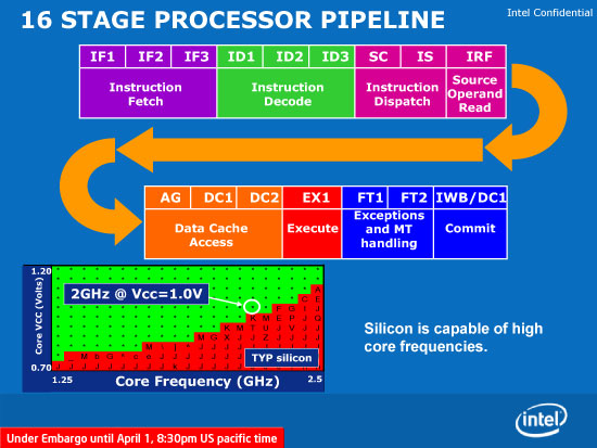
Atom's pipeline is a fairly deep 16 stages, with a 13 stage mispredict penalty. Note that this is longer than the Core 2 Duo's 14 stage pipeline, which is surprising given the low power focus the design team had for Atom.

A 16-stage pipeline complete with 3 instruction fetch and 3 instruction decode stages, more than expected
Longer pipelines are generally associated with greater power consumption especially as of late due to the Pentium 4's tenure. Intel gave us three reasons for the long pipeline:
1) Caches
2) Decoder
3) SMT
When faced with a decision between trading off latency for power, the Austin design team always favored keeping power low, even if it meant increasing latencies. Atom doesn't fire the large banks of its caches unless the cache controller knows there's a true hit in the cache, unfortunately this increases the access latency of the cache. In order to keep clock speeds high, these cache accesses have to be further pipelined. The benefit is that power is kept low; Atom keeps things as physically tagged caches to avoid the power burden of a virtually tagged cache.
The same sort of latency tradeoff is made in the decoding stages. Remember the slow vs. fast paths through the decoders? The slow path is higher latency but is guaranteed to properly decode an instruction, the added latency forces Atom to have three decoding stages instead of two.
Finally there are some algorithms in which SMT added a stage or two to the pipeline, the end result being a fairly lengthy pipeline for such a simple CPU. The reasoning however makes sense; there is no NetBurst nonsense here, all of these decisions were made to keep power consumption as low as possible while hitting the right frequency targets. As a fairly simple two-issue core, Atom needs clock speed in order to give us the sort of performance we are expecting of it.


46 Comments
View All Comments
lopri - Thursday, April 3, 2008 - link
This article is as much propagana-ish as it is technical. Did you read the last page of the article?clnee55 - Friday, April 4, 2008 - link
Since Anand wrote this article. I let him answer your accusationGulWestfale - Wednesday, April 2, 2008 - link
i believe that the graphics core in the chipset is a powerVR gen5 derivative; intel already uses some of their tech in its existing mainboards and wikipedia states that intel has licensed gen5 tech for one of its chipsets, the GMA500 (which is the same as poulsbo?) gen5 is also DX10-capable, which matches the info in your article.http://en.wikipedia.org/wiki/PowerVR#Series_5_.28S...">http://en.wikipedia.org/wiki/PowerVR#Series_5_.28S...
yyrkoon - Wednesday, April 2, 2008 - link
and wikipedia has been known to be wrong . . . a lot lately it seems.My point here *is*, I would probably trust anandtech more than wikipedia now days, as it seems any Joe can put up a 'reference' without citation.
jones377 - Wednesday, April 2, 2008 - link
Following the references link from the Wiki article...http://www.imgtec.com/News/Release/index.asp?NewsI...">http://www.imgtec.com/News/Release/index.asp?NewsI...
Poulsbo uses a PowerVR 3D core
Anand Lal Shimpi - Wednesday, April 2, 2008 - link
Yep, you guys are correct, I wasn't aware that it was public yet :) I've updated the article.Take care,
Anand